
TL;DR
ASML and Tata Electronics have signed an agreement to supply lithography equipment for India’s first front-end chip manufacturing plant in Dholera. The project, valued at $11 billion, is currently under construction and aims to begin trial production later this year.
ASML has signed a memorandum of understanding with Tata Electronics to supply lithography equipment for India’s first commercial semiconductor fab in Dholera, Gujarat, marking a major milestone in the country’s chip manufacturing efforts.
The agreement was signed during Prime Minister Narendra Modi’s visit to the Netherlands, with Dutch Prime Minister Rob Jetten present. The deal covers the deployment of ASML’s advanced lithography tools, talent development, and supply chain support for the project, which has a total investment of approximately $11 billion.
The Dholera facility is a 300mm wafer fab currently under construction, with civil works reportedly reaching about 50% completion as of last month. The project experienced a redesign late last year after soil testing revealed the ground was too soft and saline for the original structural plans. Despite this, sources indicate that the timeline remains on track, with trial production expected later this year.
Why It Matters
This development is significant because it marks India’s entry into the high-end semiconductor manufacturing sector, potentially reducing reliance on imported chips and boosting local technological capabilities. The involvement of ASML, a global leader in lithography equipment, underscores the project’s strategic importance in establishing a domestic chip supply chain.
Furthermore, the project aligns with India’s broader goal of becoming a key player in global electronics manufacturing, attracting investments, and fostering technological innovation within the country.
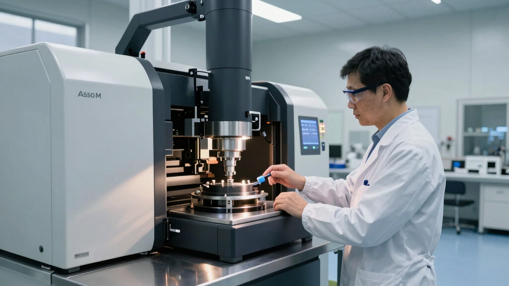
ASML lithography equipment
As an affiliate, we earn on qualifying purchases.
As an affiliate, we earn on qualifying purchases.
Background
India has been actively working to develop its semiconductor industry, with initiatives aimed at attracting global chip manufacturers and establishing domestic fabrication facilities. The Dholera project is part of this broader strategy, supported by government initiatives and significant foreign investment. The project’s progress follows earlier announcements of infrastructure development and investment commitments, with civil construction reaching the halfway mark as of last month.
ASML’s involvement is notable because its lithography tools are critical for producing advanced chips, and this marks one of the first major deployments of such equipment in India’s emerging semiconductor ecosystem.
“This partnership signals a major step forward for India’s semiconductor ambitions, especially with ASML’s cutting-edge lithography technology involved.”
— an industry analyst
“We are committed to building India’s first front-end fab with the highest standards of technology and quality, supported by our collaboration with ASML.”
— a Tata Electronics spokesperson

Semiconductor Manufacturing for the AI Era
As an affiliate, we earn on qualifying purchases.
As an affiliate, we earn on qualifying purchases.
What Remains Unclear
Details about the specific timeline for equipment deployment and the start of trial production remain unclear. It is also uncertain whether there will be further delays or technical challenges related to the soil conditions or other construction issues.
300mm wafer fab equipment
As an affiliate, we earn on qualifying purchases.
As an affiliate, we earn on qualifying purchases.
What’s Next
Next steps include completing civil construction, installing and calibrating ASML’s lithography equipment, and beginning trial production later this year. Monitoring updates from Tata and ASML will clarify progress and any potential delays.

Advanced Machining and Finishing (Handbooks in Advanced Manufacturing)
As an affiliate, we earn on qualifying purchases.
As an affiliate, we earn on qualifying purchases.
Key Questions
What is the significance of ASML’s involvement in India’s chip manufacturing?
ASML’s lithography equipment is essential for producing advanced semiconductor chips, making its involvement a major step toward establishing a high-tech, self-sufficient chip manufacturing ecosystem in India.
When is the Dholera fab expected to start trial production?
Trial production is targeted for later this year, but the exact date depends on the completion of construction, equipment installation, and calibration processes.
What challenges does the project face?
The project faced a redesign last year due to soil conditions, which could pose ongoing construction and engineering challenges, though officials say these will not delay the overall timeline.