
TL;DR

Get the latest gadgets delivered free with Prime
- Fast, free delivery on millions of items
- Prime Video, Amazon Music and more included
- Member-only deals all year
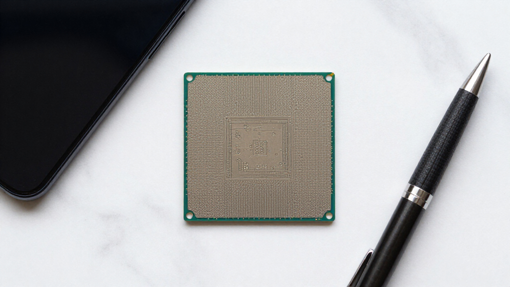
Intel has confirmed it is now shipping silicon wafers produced using high-NA EUV lithography technology. This development signals progress in advanced semiconductor manufacturing, potentially impacting future chip performance and supply chains.
Intel has confirmed it is now shipping silicon wafers produced with high-NA EUV lithography technology, marking a key milestone in advanced chip manufacturing. This development positions Intel at the forefront of semiconductor fabrication, potentially enabling more powerful and energy-efficient chips. The move is significant for the industry, as high-NA EUV has been a critical but challenging technology to implement at scale.
According to Intel, the company has begun shipping silicon wafers manufactured using high-NA EUV (extreme ultraviolet) lithography equipment, which allows for finer patterning at smaller nodes. This technology has been under development for several years, with high-NA EUV systems introduced by equipment suppliers like ASML as a next-generation tool for leading-edge chip production. Intel’s announcement confirms that it has successfully integrated high-NA EUV into its fabrication process, moving beyond initial pilot phases.Sources familiar with Intel’s manufacturing plans indicate that the company is now shipping wafers at the Intel 3 process node, which leverages high-NA EUV for critical layer patterning. This process node is expected to deliver performance improvements and power efficiency gains over previous generations, such as Intel 4. The shipments are reportedly targeted toward high-volume manufacturing for Intel’s upcoming products, with plans to expand use of high-NA EUV to other nodes in the future.
Impact on Semiconductor Manufacturing and Industry Leadership
This milestone signifies that Intel has overcome key technical challenges associated with high-NA EUV lithography, which has been regarded as essential for continuing Moore’s Law and scaling down transistor sizes. The ability to ship wafers at this advanced node enhances Intel’s competitive position against rivals like TSMC and Samsung, who are also investing heavily in EUV technology. It could lead to faster deployment of next-generation chips, influencing supply chains and market dynamics.
As an affiliate, we earn on qualifying purchases.
High-NA EUV: A Critical Step in Advanced Chip Fabrication
High-NA EUV lithography systems, developed by ASML, are considered a breakthrough for pushing the limits of semiconductor miniaturization. Unlike earlier EUV systems, high-NA tools feature a higher numerical aperture, enabling finer patterning at smaller nodes such as 3nm and below. The technology has faced numerous technical hurdles, including equipment complexity, mask defects, and process stability. Leading chipmakers like TSMC and Samsung have been testing high-NA EUV for several years, with production ramp-up expected soon.
Intel’s move to ship wafers using high-NA EUV indicates that it has successfully integrated this technology into its manufacturing line, following earlier pilot and development phases. The company announced its intention to adopt high-NA EUV for its next-generation nodes last year, aiming for a competitive edge in performance and power efficiency.
“We are now shipping silicon wafers produced with high-NA EUV lithography, marking a significant milestone in our manufacturing evolution.”
— Intel spokesperson
Intel 3 process node semiconductor wafers
As an affiliate, we earn on qualifying purchases.
As an affiliate, we earn on qualifying purchases.
Extent of High-NA EUV Adoption and Future Plans
While Intel confirms it is now shipping wafers with high-NA EUV, it is not yet clear how extensively the technology will be adopted across all manufacturing nodes or the timeline for full-scale deployment. Details on the volume of wafers produced, cost implications, and whether this will immediately impact product availability remain undisclosed. Additionally, the performance and yield metrics associated with high-NA EUV at scale are still emerging.
extreme ultraviolet lithography tools
As an affiliate, we earn on qualifying purchases.
As an affiliate, we earn on qualifying purchases.
Next Steps in High-NA EUV Deployment and Industry Impact
Intel is expected to expand the use of high-NA EUV to additional process nodes in the coming months, with plans to ramp up production volumes. Industry observers will monitor how quickly other chipmakers adopt this technology and how it influences market competition. Intel’s upcoming product launches, likely featuring chips manufactured with high-NA EUV, will serve as key indicators of the technology’s impact.
advanced semiconductor manufacturing equipment
As an affiliate, we earn on qualifying purchases.
As an affiliate, we earn on qualifying purchases.
Key Questions
What is high-NA EUV lithography?
High-NA EUV lithography is an advanced manufacturing technology that uses extreme ultraviolet light with a higher numerical aperture to create finer patterns on silicon wafers, enabling smaller, more powerful chips.
Why is this development important for Intel?
Shipping wafers with high-NA EUV indicates Intel has achieved a key milestone in process technology, which can lead to better performance, power efficiency, and competitiveness in the semiconductor industry.
When will high-NA EUV be used in mass production?
Intel has begun shipping wafers now, but full-scale adoption across all product lines is expected to ramp up over the next few quarters, with broader industry adoption likely in the next 1-2 years.
How does high-NA EUV compare to previous lithography methods?
High-NA EUV allows for finer patterning at smaller nodes than earlier EUV systems, enabling continued miniaturization and performance improvements beyond what was previously possible.
What are the technical challenges remaining with high-NA EUV?
Challenges include equipment complexity, mask defect control, process stability, and cost. While Intel has achieved initial shipping, scaling to full production remains a technical and economic challenge for the industry.
Source: hn
Halloween Picks
halloween
As an affiliate, we earn on qualifying purchases.